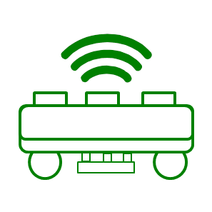
Innovative Technology
Bumping
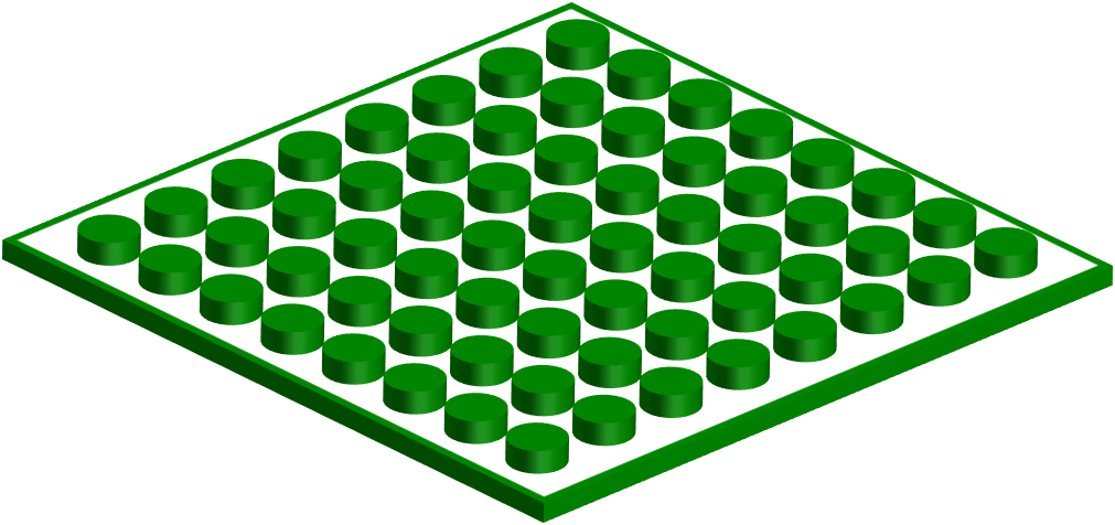
Wafer bumping is a metal bump that grows on a wafer, and each bump is an IC signal contact. Unlike conventional interconnection through wire-bond, bond pads are placed at peripheral area , IO pads for bumping could be distributed all over the surface of the chip, thus chip size could be shrunk and electrical path could be optimized. The growth of smaller form factor and high performance package are deriving bumping more popular to replace traditional wire-bond package.
Bumping
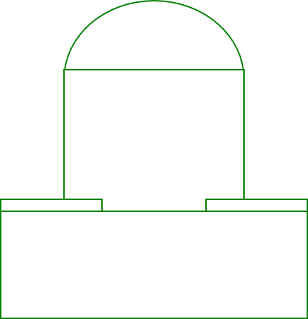
Solder Bump
Bumping is replacing wire bonding as the connecting method to accommodate the growing number of components. Out of all the bumping types, lead-free bumping has the longest production history in flip chip technology. Lead-free bumps are spheres of solders, which are formed on contact pads of semiconductor devices and subsequently used in flip chip bonding.PTI start mass production since 2013.
Capability
- Bump pitch 130~250 um
- Bump height 70~100 um
- Optional PI layer for logic and memory device
Bumping
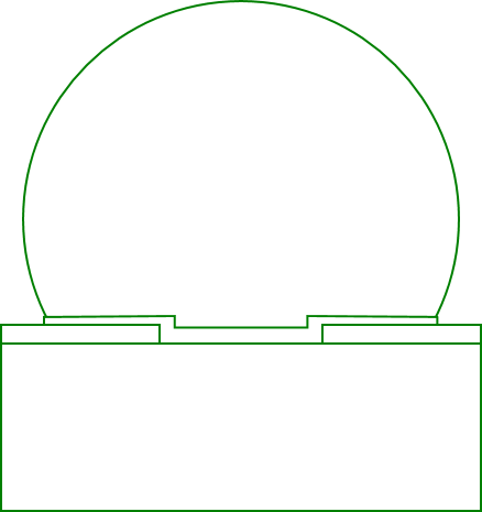
Cu Pillar Bump
The Copper Pillar Bump (CPB) structure exhibits improved electron-migration resistance, reduces power loss and signal delay, better heat dissipation performance . CPB technology also provides great control of joint diameter and stand off height compared with solder bump , enabling the creation of fine pitch joint. The application could be Mobile AP ,HPC,Baseband ,memory ,ASIC and SOC. PTI has production experience Since 2013, including various logic and memory devices.
Capability
- Bump pitch 40~130 um
- Max bump height 103 um
- Optional PI layer for logic and memory device
Bumping
RDL Solution
CuNiAu redistribution layer (RDL) is mainly used in packaging technologies that require high corrosion resistance, high reliability, and good solderability, as the Au surface can reduce oxidation and provide low-loss signal transmission. Cu RDL is primarily applied in high-density, high-performance, and cost-effective advanced packaging, enhancing I/O density and reducing package size.
Capability
- Cu & Cu/Ni/Au RDL
- Min Line/space : 5/5 um
- Available structure: 2P1M ,2P2M & 3P2M